Classification of Field Effect Transistors
1. Field effect transistors are divided into junction field-effect transistors (JFETs) and metal oxide semiconductor field-effect transistors (MOSFETs);
2. Junction field-effect transistors (JFETs) are divided into two types: N-channel and P-channel, which are relatively rare in practical applications;
3. MOSFETs can be divided into two categories: enhancement type and depletion type, each of which can be divided into NMOS and PMOS; The most commonly used on general motherboards are enhanced MOS transistors, NMOS transistors, which are mostly used for signal control, followed by PMOS transistors, which are mostly used for power switches, and depletion transistors are almost not used.
Two Field Effect Transistor Structure
A MOS transistor has three poles: gate, drain, and source. Typically, the substrate of a MOS transistor is connected to the S pole inside the transistor, and there is usually a parasitic diode between the D and S poles; Whether it is an N-channel or a P-channel, the direction of the parasitic diode is always consistent with the direction of the arrow; The schematic diagram of N/P channel field-effect transistor is as follows:
Parasitic diode, also known as body diode, is like a regular diode. When connected positively, it conducts, and when connected negatively, it turns off. For NMOS, when the S pole is connected positively and the D pole is connected negatively, the parasitic diode conducts, and vice versa; For PMOS transistors, when the D terminal is connected to positive and the S terminal is connected to negative, the parasitic diode conducts, and vice versa. In some application scenarios, body diodes are also chosen to increase the voltage drop between DS (the voltage drop of body diodes is much larger than the conduction voltage drop of MOS), while also paying attention to the overcurrent capability of body diodes. When the conduction conditions of the MOS transistor are met, the D and S poles of the MOS transistor will conduct, and the body diode will be in the off state. This is because the conduction internal resistance of the MOS transistor is extremely small, usually at the level of m Ω, and the current flowing through 1A level is only at the level of mV. Therefore, the conduction voltage drop between the D and S poles is very small, which is not enough to make the parasitic diode conduct. This requires special attention.
Simple Application of Three Field Effect Transistors
Field effect transistors belong to voltage controlled devices. For enhanced MOS transistors, when VGS is greater than a certain value, the transistor will conduct. Here, the "certain value" refers to the turn-on voltage VGS (th).
Difference between 4 and transistor
The difference in switch speed. When a transistor is working, both PN junctions will induce charges. When the switching transistor is in a conducting state, the transistor is in a saturated state. Assuming that the transistor is turned off at this time, the charges induced by the PN junction need to be restored to a balanced state, which takes time. Due to its different working modes, MOS does not require recovery time, so it can be used as a high-speed switching transistor. The control methods are different. MOS transistor is a voltage control element, while transistor is a current control element. When only allowing a small amount of current to be drawn from the signal source, MOS transistors should be selected; When the signal voltage is low and more current is allowed to be drawn from the signal source, a transistor should be selected. The number of types of conductive carriers varies. The unipolar devices mentioned in power electronics technology refer to devices that rely solely on one type of carrier to conduct electricity, while bipolar devices refer to devices that rely on two types of carrier to conduct electricity. MOS transistors are also known as unipolar devices because only the majority of charge carriers participate in conduction; The transistor is called a bipolar device because both the majority and minority carriers participate in conduction. Different integration capabilities. MOS transistors can operate under very low current and voltage conditions, and their manufacturing process can easily integrate many MOS transistors on a single silicon wafer. Therefore, MOS transistors have been widely used in large-scale integrated circuits. The input impedance and noise capability are different. MOS transistors have the advantages of high input impedance and low noise, and are widely used in various electronic devices. 6. The cost of MOS transistor is higher than that of transistor. Based on the characteristics of the two components, MOS transistor is commonly used in high-frequency and high-speed circuits, high current places, and central areas that are sensitive to base or drain control current; And the transistor is used in low-cost places.
5 series resistor function
1、 The role of series resistance between G and S poles
The input impedance of MOS transistor is very high, and it is easily affected by external signal interference. With a small amount of charge, a high voltage can be generated at both ends of the equivalent capacitance between G-S poles. If the charge is not released in time, the high voltage at both ends can easily cause MOS transistor to malfunction, and even break down the G-S pole. Connecting a resistor in series between G and S poles can prevent static electricity from damaging MOS.
Providing a fixed bias ensures that the MOS is effectively turned off when the front pole is open.
2、 The function of the G-pole series resistor is to slow down the rate of change of Rds from infinity to Rds (on).
To prevent oscillation, the I/O output ports of general microcontrollers may carry some stray inductance. In the event of a sudden voltage change, it may form LC oscillation with the gate capacitor. Series resistance can increase damping and reduce oscillation effects.
Reduce the peak current of gate charging.
6 Selection Points
1. Voltage value
The maximum withstand voltage VDS between D-S and the maximum withstand voltage VGS between G-S should not exceed these two values during actual use to avoid damaging the MOS transistor.
To turn on the voltage VGS (th), MOS transistors are generally controlled by microcontrollers. The appropriate conduction threshold MOS transistor is selected based on the level of the microcontroller, and a certain margin is left as much as possible to ensure that the MOS can switch normally.
2. Current value
It represents the current that can flow through the MOS transistor and its ability to reflect the load. Beyond this value, the MOS transistor will also be damaged.
3. Power loss
Power loss includes thermal resistance and temperature. Thermal resistance refers to the ratio between the temperature difference between the two ends of an object and the power of the heat source when heat is transferred to the object. The unit is ℃/W. The formula for thermal resistance is R θ JA=(Tj Ta)/PD.
4. Conducting impedance
The smaller the conduction impedance, the smaller the loss of the MOS transistor. Generally, the conduction impedance of MOS transistors is in the m Ω range.
5. Switching time
In high-speed circuits, it is advisable to choose MOS transistors with small input and output capacitors Ciss&CoSs and short switching times Ton&Off to ensure normal data communication.
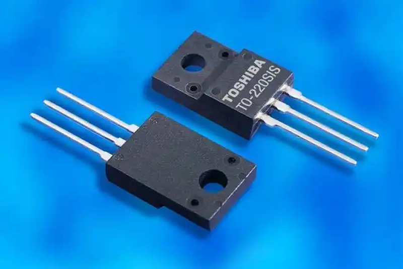
6. Packaging
According to the size of the PCB board, choose the appropriate MOS transistor size, and in the case of limited board area, try to choose small packages as much as possible; For medium and low voltage low power, you can choose our SOT-23, SOT-23-3/6, and SOT-89 packages, while for high power, you can choose our DFN/QFN series packages.
 Language

 Your location:


 Follow us
 Tel: 400-665-0769
 E-mail